Hot Sales
 Memory - Modules, Cards
  Integrated Circuits (ICs)
  RF and Wireless


News

TC58BVG1S3HTAI0 Complete Datasheet: 2Gb SLC NAND Pin Definition, Timing Diagram and Equivalent Selection Guide
TC58BVG1S3HTAI0, as a classic 2Gb SLC NAND Flash device from Kioxia (formerly Toshiba Memory), is still widely used in industrial control, network communications, automotive electr…
TC58BVG0S3HTAI0 Data Sheet Read: 1Gbit SLC NAND Key Parameters and Design Considerations
SLC NAND 1Gbit Industrial Grade KIOXIA In a typical embedded system, non-volatile storage can account for 10%-15% of the cost. As a mature 1Gbit SLC NAND Flash for industrial appli…

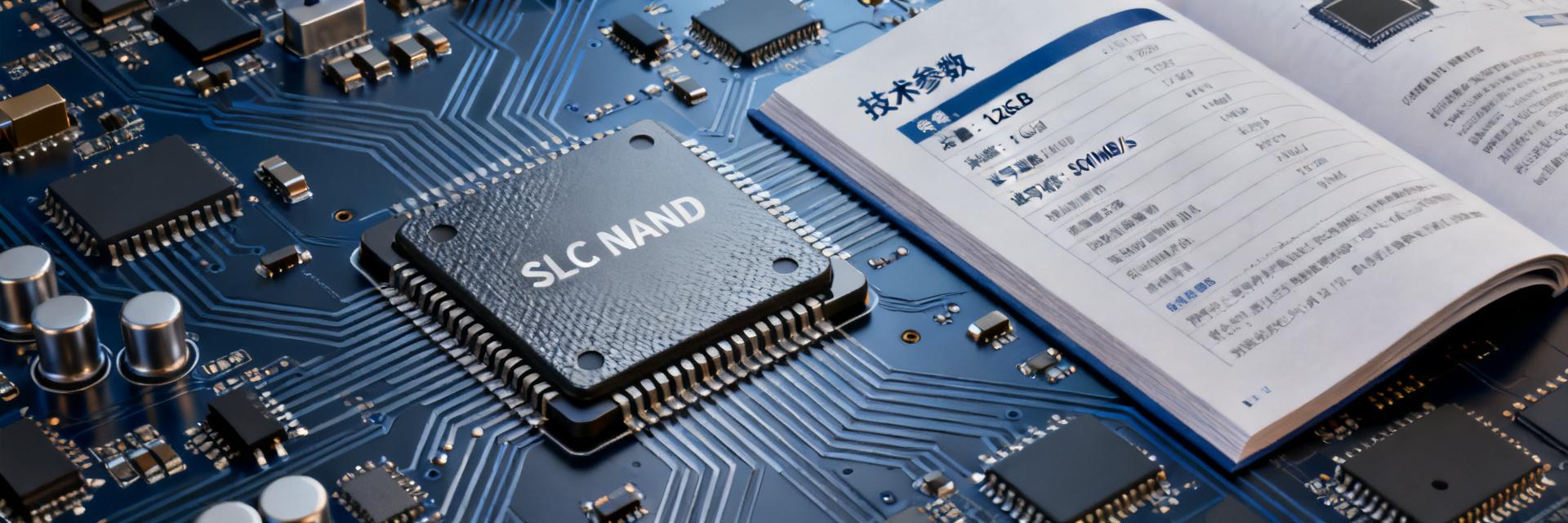
TC58BVG0S3HTA00 Data Sheet 1 Picture Memory: All Key Specifications of 1 Gbit SLC NAND
At storage selection meetings for domestic industrial controllers, automotive T-Boxes, and AI IPCs, the most common question engineers ask is: "If I only remember one image, which …
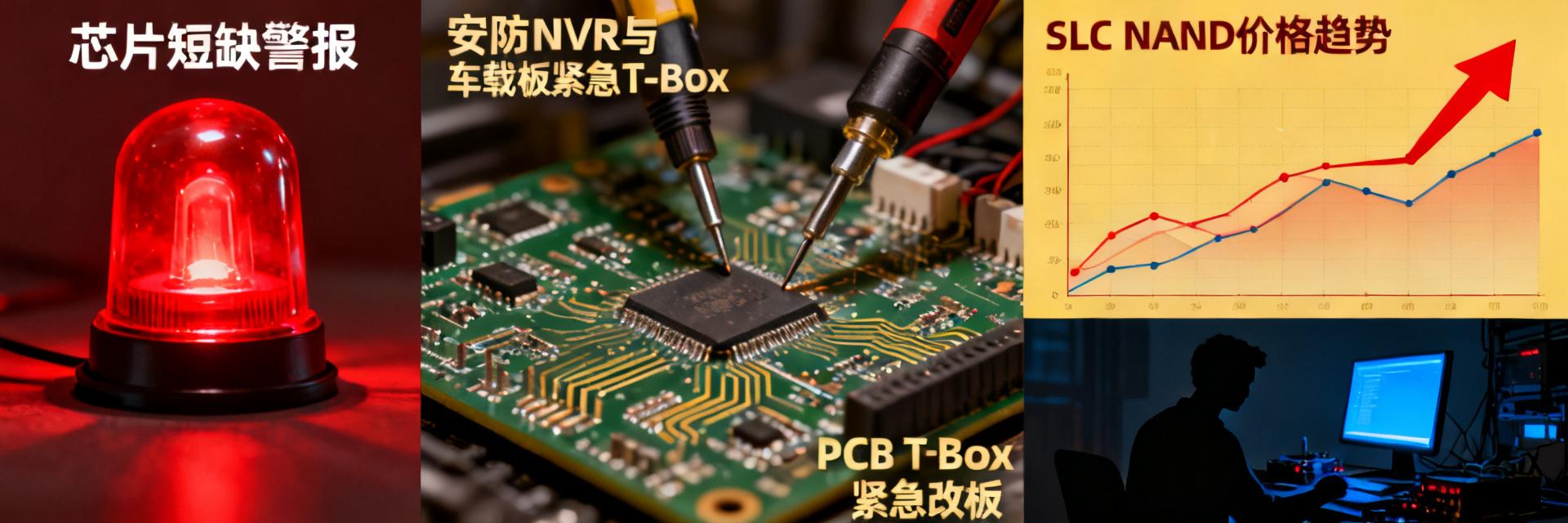
From Security to Automotive: Real Cases and Response Strategies of Two Chinese Manufacturers Forced to Change Schemes Due to SLC NAND Price Increases
In-depth Case Study Published: April 2025 Reading Time: 8 minutes "A 280% surge—we were forced to revise our schematics overnight." —— This is a quote from a security hardware dire…
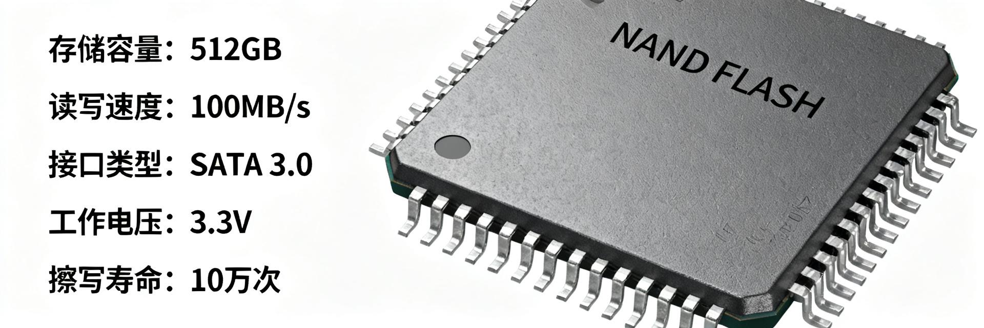
TC58BVG0S3HBAI6 Data Sheet Deep Analysis: 5 Key Parameters and Selection Guide
As the demand for high reliability and small-footprint storage in embedded systems continues to grow, requirements for storage chips in industrial control and the Internet of Thing…
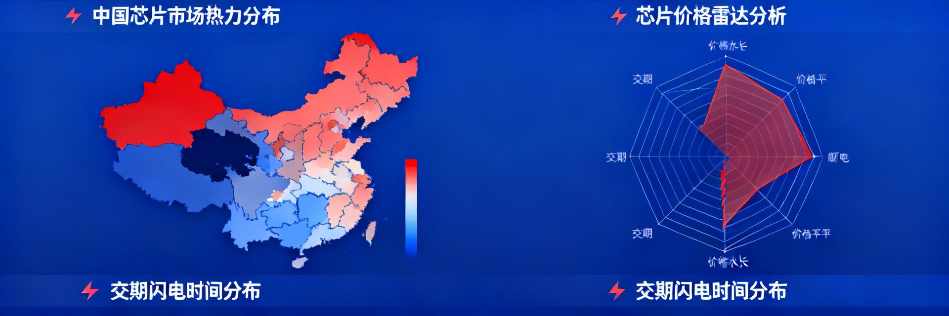
TC58BVG0S3HBAI4现货 Price Map: 2025 Latest Channel Data + Lead Time Radar Chart
“Spot 5.73 RMB, Lead Time 3-6 Weeks” — The price and lead time of TC58BVG0S3HBAI4 have fluctuated like an EKG over the past 90 days. If you are struggling with the procurement plan…
